Currently, my research is about single photon emitters based on atomic defects of hexagonal boron nitride (h-BN) under supervision of professor Harry Atwater at Caltech. Single photon emitters (as can be inferred from the name) are emissive species which can emit single photons on demand. They are the building blocks of future quantum communication technologies and they already have applications in random number generation and quantum sensing.
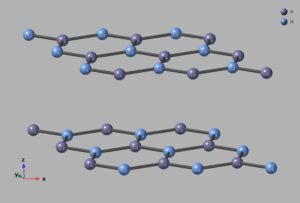
hexagonal Boron Nitride (h-BN) is a part of layered Van der Waals (2D) materials family which means we can exfoliate a single atomic layer of this material. a single photon emitter in a 2D sheet of atoms is an interesting idea which can lead to novel applications and a rich science, for example the emitter-phonon interaction can be very interesting.
We have studied the mechanisms which cause broadening of emission line in these emitters and the results are published here .we could identify sources of broadening and propose a method to suppress inhomogeneous broadening of emitters at 4 Kelvin.
We Also could probe the position and orientation of emitter dipole in bulk h-BN by engineering the Local Density of Optical States (LDOS) with a phase change material. you can find the preprint on arXiv. our result shows that the direction of emitter dipole is mainly out of plane and, our technique is able to extract the height location of emitter with sub diffraction limit precision.
During my masters I worked on perovskite solar cells under supervision of professor Nima Taghavinia at Sharif university of technology (Tehran-Iran). I was mostly working on printing mechanisms of photo-voltaic devices. we designed and fabricated a printer to print semiconductor films. you can see the result in this publication.